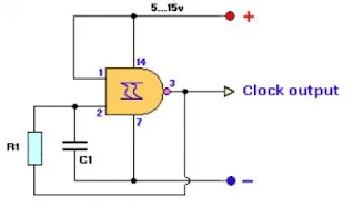
NAND Gate Clock Generator Circuit
1. Working Principle
This circuit uses two NAND gates configured as an oscillator:
R1 and C1 determine the frequency
The third gate buffers the output
Works with 5-15V (CMOS 4011) or 5V (TTL 7400)
2. Basic Circuit Diagram
 +Vcc
  |
  R1 (100K)
  |-----> Gate 1 (Input A)
  |
 C1 (10nF)
  |
 GND
Output: Gate 3 (pin 3 on 4011)
3. Frequency Calculation
Approximate formula:
f ≈ 1 / (2.2 × R1 × C1)
Examples:
R1=100K, C1=10nF → f ≈ 454Hz
R1=1M, C1=100nF → f ≈ 4.54Hz
4. Component Selection
| Component | Value Range |
|---|---|
| R1 | 10KΩ - 10MΩ |
| C1 | 100pF - 47μF |
| Power | 5-15V (CMOS) |
5. IC 4011 Pinout
  ___ ___
1|   U   |14  Vcc
2|       |13
3|       |12
4|       |11
5|       |10
6|       |9
7| GND   |8
6. Practical Applications
Clock source for 4017 counters
Circuit timing control
Test signal generator
Educational digital systems
7. Implementation Tips
✔ Use ceramic or polyester capacitors for better stability
✔ Add a 1MΩ potentiometer in series with R1 for fine tuning
✔ Include an output buffer for heavy loads
Precision Variation
For more stable output:
Replace R1 with 1MΩ potentiometer + 100K resistor
Use polypropylene capacitors for critical timing
Pro Tip: This simple yet effective circuit is perfect for learning digital electronics. The CMOS version (4011) offers wider voltage range than TTL (7400).
Need higher stability? Consider crystal oscillator circuits!
#DigitalElectronics #ClockGenerator #CMOS4011 #ElectronicsProject #LogicOscillator #FrequencyControl


